


Welcome to Tesla Motors Club
Discuss Tesla's Model S, Model 3, Model X, Model Y, Cybertruck, Roadster and More.
Register
Install the app
How to install the app on iOS
You can install our site as a web app on your iOS device by utilizing the Add to Home Screen feature in Safari. Please see this thread for more details on this.
Note: This feature may not be available in some browsers.
-
Want to remove ads? Register an account and login to see fewer ads, and become a Supporting Member to remove almost all ads.
You are using an out of date browser. It may not display this or other websites correctly.
You should upgrade or use an alternative browser.
You should upgrade or use an alternative browser.
Potential Tesla Semiconductor Fab Plant
- Thread starter Buckminster
- Start date
adiggs
Well-Known Member
A link to my post over in the main thread. I was writing the post as this thread was being created.
 teslamotorsclub.com
Tesla, TSLA & the Investment World: the Perpetual Investors' Roundtable
Elon tweeted large pouch cells are dangerous. . This is as evident by the GM Bolt recall due to fire and explosion. I’m not sure how many OEMs are using this form factor but perhaps many. Like I have said before, quoting Linus Torvalds: Those who don’t understand Teslas are condemned to...
teslamotorsclub.com
FAB or not a FAB? Let's get the terms right at least.
In Semiconductors, the FAB only creates the silicon wafer part which is an array of repeat circuits called Die. But it is not the package, and not the circuit boards that they mount onto for connection to other chips. The room with the yellow lights and bunnysuits, that's the FAB, short for Fabrication of the Wafer. I should know, I used to design and teach process courses at Intel and still have class samples from early days. I don't have a 4004 chip, that's just too cool and the one on Voyager still running today!
Assembly and Test (A/T) simply protects and provides connections (that you can see) to form an actually chip you can buy. Cost for A/T factories are much lower than FABs. Since A/T is the bu** hole without a real budget, and some at Intel refer to the FAB as the "Factory" (dismissing A/T as any factory), most foundary companies can do this without too much trouble. It's low-tech mostly, and done wherever labor is cheap. But the FABs are protected so very different factories, locations, costs. Intel and other majors have their own A/T. But let's be clear, FAB has the super high $10B entry price and is changing fast (hasn't stopped). The race is (has been) for speed, power, and cost. Shrink a circuit and it will use less power and run faster clocks. Drop the voltage down and even more energy is saved. (Wasn't dojo down in the 1V range?)
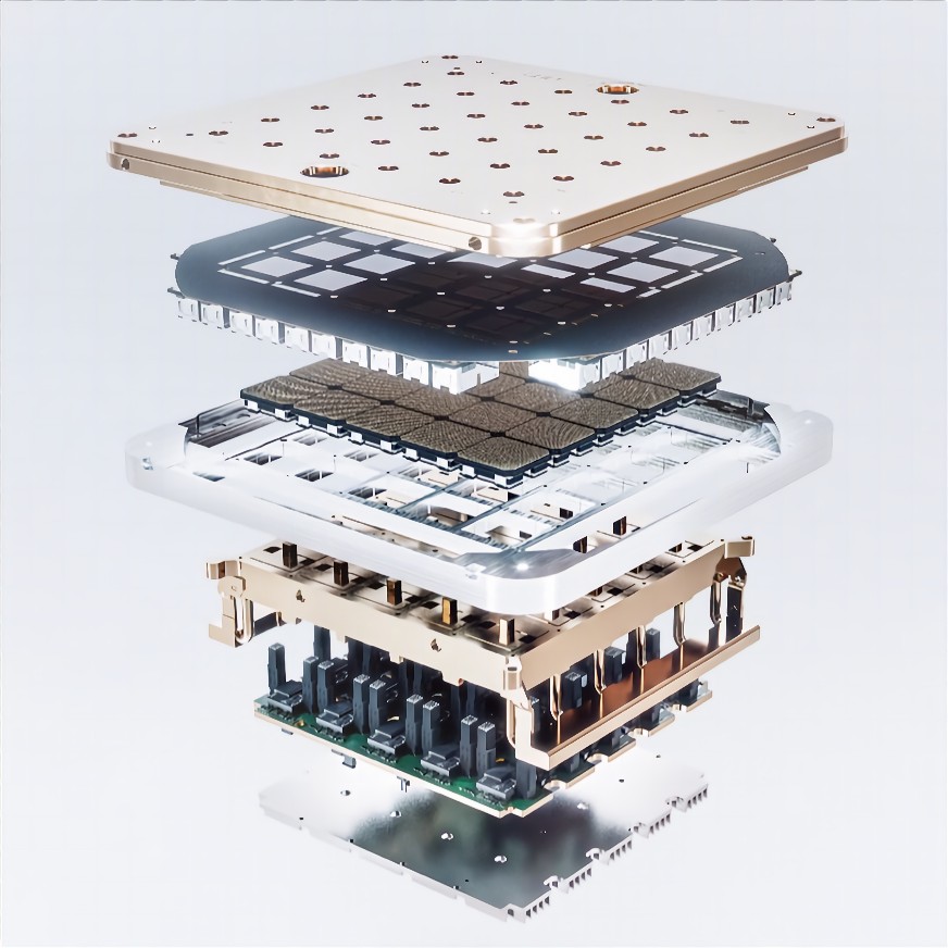
Earliest new chip releases happen on the larger packages for heat dissipation until it can be shrunk and run cooler for laptops etc. From the size of the Dojo's cooling system, this must be creating a lot of heat! So they have 25 Die on a substrate that the world has never seen before. I'm not sure if it was mentioned, but the comment about "Dojo maintains bandwidth even when adding on more modules" caught my interest. I think the bus is using light. (Can anyone confirm this?). The connections to the die go into a bunch of devices around it, but there are no wires or boards showing. I doubt the die are connected edge-wise (would be truely amazing) so there must be connections (as usual in the form of thousands of solder bumps) on the underside of each chip. But this one comment on not losing bandwidth across several feet of space has me curious if they didn't introduce fibre optics for the connections. I mean, what if the die are projecting data upwards off the chip as light, and the backside is simply for power and cooling? Hmm... (Now I'm dreaming up stuff.)
In Semiconductors, the FAB only creates the silicon wafer part which is an array of repeat circuits called Die. But it is not the package, and not the circuit boards that they mount onto for connection to other chips. The room with the yellow lights and bunnysuits, that's the FAB, short for Fabrication of the Wafer. I should know, I used to design and teach process courses at Intel and still have class samples from early days. I don't have a 4004 chip, that's just too cool and the one on Voyager still running today!
Assembly and Test (A/T) simply protects and provides connections (that you can see) to form an actually chip you can buy. Cost for A/T factories are much lower than FABs. Since A/T is the bu** hole without a real budget, and some at Intel refer to the FAB as the "Factory" (dismissing A/T as any factory), most foundary companies can do this without too much trouble. It's low-tech mostly, and done wherever labor is cheap. But the FABs are protected so very different factories, locations, costs. Intel and other majors have their own A/T. But let's be clear, FAB has the super high $10B entry price and is changing fast (hasn't stopped). The race is (has been) for speed, power, and cost. Shrink a circuit and it will use less power and run faster clocks. Drop the voltage down and even more energy is saved. (Wasn't dojo down in the 1V range?)
Earliest new chip releases happen on the larger packages for heat dissipation until it can be shrunk and run cooler for laptops etc. From the size of the Dojo's cooling system, this must be creating a lot of heat! So they have 25 Die on a substrate that the world has never seen before. I'm not sure if it was mentioned, but the comment about "Dojo maintains bandwidth even when adding on more modules" caught my interest. I think the bus is using light. (Can anyone confirm this?). The connections to the die go into a bunch of devices around it, but there are no wires or boards showing. I doubt the die are connected edge-wise (would be truely amazing) so there must be connections (as usual in the form of thousands of solder bumps) on the underside of each chip. But this one comment on not losing bandwidth across several feet of space has me curious if they didn't introduce fibre optics for the connections. I mean, what if the die are projecting data upwards off the chip as light, and the backside is simply for power and cooling? Hmm... (Now I'm dreaming up stuff.)
MC3OZ
Active Member
IMO Tesla might start by buying a company that owns a number of older FABs and target lower tech commodity automotive chips..But let's be clear, FAB has the super high $10B entry price and is changing fast (hasn't stopped). The race is (has been) for speed, power, and cost.
My rationale is needing high volumes of these chips, and the ability to improve the designs within the scale that the factory can support... probably something like 10 nm,.
Or Tesla might be happy to simply contract supply, or go into a joint venture...
IMO if we could establish a good reason why should Tesla build a FAB, the costs and the technical difficulties would not stop them.
To confirm this one way other the other we would need to know their product plans car, robots and anything else they might be doing...
I don't think they will necessarily stop at cars and robots...and that might change all calculations on how many chips they need.
While the order of magnitude might be different, I see this as a similar decision to in house battery supply..
The decision to manufacture batteries was taken because Tesla could not be sure suppliers could supply the volumes they needed at the price they wanted.
The decision to build a higher end FAB really requires a strong need for products which Tesla doesn't think others can supply at the right prices, or in the right volumes... At present, to the best of our knowledge, we don't know of a pressing need to build a FAB.
What we do know is Elon thinks ahead, plans ahead and often projects fly under the radar... If there was a project, my guess is at this stage they are just evaluating buying an company that owns one or more older FABs. I doubt they would build a state-of-the-art FAB from scratch with no prior experience in the industry... When you buy a company, a team of experienced people come with the package, many of which should be happy to stay.
MC3OZ
Active Member
Here is another related thread and a background video that I linked;- Semiconductor Shortage and Car Production
 teslamotorsclub.com
Overall it still looks like US FABs will reduce the dependency on the TSMC Taiwan factories and the local water supply..
Semiconductor Shortage and Car Production
https://www.autoevolution.com/news/chip-shortage-might-turn-into-market-saturation-analysts-worry-166666.html ... chip manufacturers have responded to increasing demand with investments in new capacity. Once those investments will be completed and supply will slowly, but surely, meet demand...
teslamotorsclub.com
Overall it still looks like US FABs will reduce the dependency on the TSMC Taiwan factories and the local water supply..
I’ll leave it to those knowledgeable in the semiconductor/FAB/chip/AT and so forth production sector to keep this an active and productive thread. For starters: please provide insight as to what your opinions are regarding Samsung and the Taylor, TX news released over the past days; specifically, what is it - and WHEN -might $17 billion provide, most particularly to Tesla?
For starters: please provide insight as to what your opinions are regarding Samsung and the Taylor, TX news released over the past days; specifically, what is it - and WHEN -might $17 billion provide, most particularly to Tesla?
Here is an article on it:
Tesla supplier Samsung is building a $17B chip factory 40 mins away from Giga TX
Tesla key supplier Samsung Electronics has reportedly selected Taylor, TX, as the site of its upcoming $17 billion chip plant. The company is reportedly set to meet with the city’s authorities on Wednesday to discuss the new facility’s construction details. The update was posted at the Korea...
 www.teslarati.com
It seems that isn't expected to open until the end of 2024.
2-3 years for spending $17billion. That may or may not be the case: perhaps it opens for initial production after a mere $2-3 billion has been spent - I’ve no idea - but none of those metrics differ substantially from the kinds of expenditures and timetables Tesla has been demonstrating.
adiggs
Well-Known Member
Pretty much spend it all to get the first unit, unless what they're actually doing is building more of a fab complex (many cleanrooms). It's really the cleanroom at the heart of it that defines a fab. Those cleanrooms are getting bigger and bigger which is the primary driver of fab cost. Well - that and the tools that can be 2 stories tall (small - medium sized house isn't a bad mental model for some of them) and need MW+ power supplies - those are expensive too2-3 years for spending $17billion. That may or may not be the case: perhaps it opens for initial production after a mere $2-3 billion has been spent - I’ve no idea - but none of those metrics differ substantially from the kinds of expenditures and timetables Tesla has been demonstrating.

If they're getting 1 really big cleanroom out of that, then a good mental model is to spend it all to get ready to manufacture the first unit.
It's a lot cheaper if this isn't cutting edge. I.e. 3 or 4 nodes back - 1 and 2 nodes back are still being used for high performance parts. But 3 or 4 nodes back won't work for the training and inference chips we're all so excited about. They would work well for the anti-lock brake controllers and similar though.
The quantity of money between Tesla investment and this Fab network might be comparable - the units though make the economics orders of magnitude different. Units are worth pennies and dollars (some of the big server parts can get into 000s of dollars, but not nearly as many / wafer) for fabs. For Samsung / manufacturer, I believe that what they're actually selling are wafer starts, with the customer 'paying' for the packaging and yield at the end (80% yield means the customer got 80% of the theoretical max from the wafer). I don't know what wafers go for though.
To make the economics work for the manufacturer, you need a LOT of unit volume. So much that Samsung, with all of the semiconductors they consume internally, can't keep their factories sufficiently busy on their own - they need to sell wafer starts to others as well. Of course they've also built a business around making parts for others, so that's an important reason for their network being so large.
The only company I know of that makes and consumes all of its own parts is Intel (within a rounding error). If you want a first order approximation of the size of expenditure and revenue / unit volume to make a fab work (as well as profitability, and making it profitable), look at Intel and it's financials. That isn't $17B for a factory - that's $17B/year for factories, upgrades to the factories, and another similar amount for R&D on fab technology. I'm pretty sure that most of that is the tools in the factory - not the building and cleanrooms themselves. Tesla could cut back on that - maybe 1/2 of each, but maybe not. Like car manufacturing there is a disproportionate gain in profit as you scale up, as well as a minimum amount to earn as much as you spend.
Tesla wasn't particularly profitable with 1 factory (Fremont). It's becoming wildly profitable with 2, with 2 more on the way expected to make things ridiculous. I doubt the economics would work with a single fab, and probably not with 2 or 3, where 'work' = enough revenue to pay for the capital and R&D.
As a Tesla investor, the case for a fab network that is designed to break even would have a lot of explaining how that benefits the business. And a fab network that can be similarly profitable as the rest of the business would need a lot of explaining about where the unit volume comes from, it's value, and the R&D expenditures Tesla will need to get started and how Tesla is going to make enough of that to stay up with and even push the leading edge of the technology.
adiggs
Well-Known Member
So I barely understand this stuff, but I did some a moderate study (a few days worth) of 1 single technology that goes into a fab. The (or at least a) big holdup on the very newest nodes has been Extreme Ultraviolet technology. At a simplistic view of things, a wafer is patterned by shining a bright flashlight on it with the right photoresist in order to print the circuitry. (Really, really simplistic).
This next technology is a much smaller wavelength of light that will print smaller lines.
So, we need an EUV flashlight. But we don't need any EUV flashlight - we need a very specific wavelength. Other wavelengths are bad and need to not be generated, or need to be filtered out.
The way I understand this - to generate that light you have a tool that shoots a drop of molten tin into a chamber. A laser of the right kind blasts that droplet of tin to shape it right, and then blasts it again, to make just that right wavelength of light.
You don't get a laser out of that - you get something that goes all over the place. You need to gather that light up and turn it into a flashlight - get em all going in roughly the same direction. And you want the other residual particles to stay out of it so they don't get to the wafer and mess things up (so the tools need to be cleaned regularly). That gets into a lot of the other technical problems - we're a long ways away from a tool that can print a wafer.
Shockingly I know, this is hard enough that the distance from theory, lab, to production was longer than expected. The big deal wasn't that we couldn't do it many years ago - the big deal was that a tool with a MW power supply could deliver something like 150-200 watts to the wafer and to make it work at production scale and economically it needed to be more like 300 watts (more is better - exposure time goes down, therefore units/time are higher).
These tools are an example of that 2 story / small house sized tools with MW power supplies.
I have no idea what the research science boffins are working on next, but I do know that when you're counting atoms in your lines and worrying about whether there will be enough of them, it won't be anything resembling easy.
Or magic - that's what I say!
Take none of this as a a good enough description to keep somebody that really understands it from rolling on the floor with laughter or the numbers as correct. Take this as being directionally accurate and the best that a layperson was able to understand from some technical articles that I needed to read for other purposes.
OR: Extreme ultraviolet lithography - Wikipedia
Similar threads
- Replies
- 74
- Views
- 6K
- Replies
- 3
- Views
- 486
- Replies
- 5
- Views
- 1K
- Replies
- 3
- Views
- 1K