

Hello All-
Today I was reading the following thread (which is wonderful by the way) about the known and unknown properties of the HW2 camera suite. I suggest you read it if you're into highly technical stuff:
AP2.0 Cameras: Capabilities and Limitations?
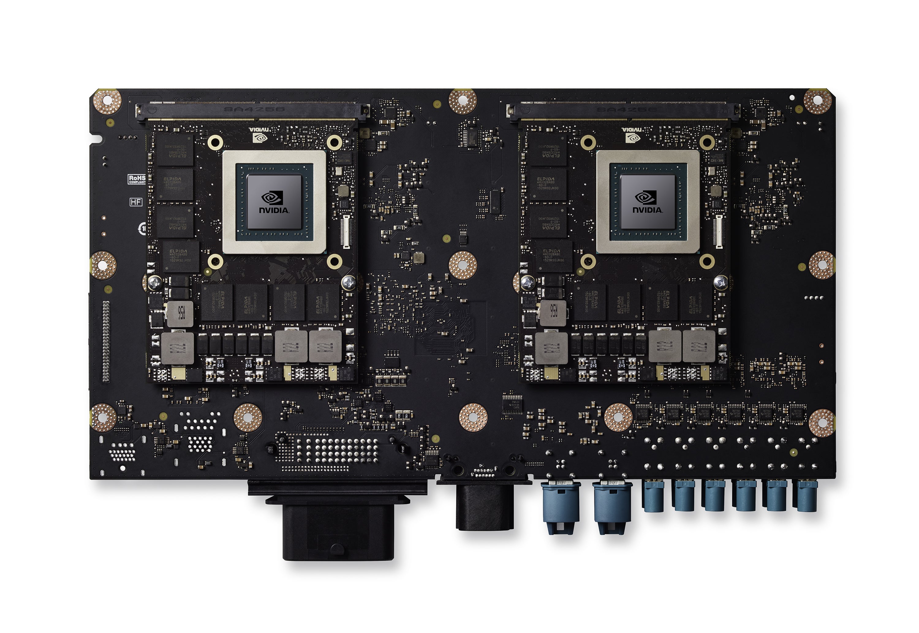
However, even after seven months since release, nobody has decided to disassemble the new NVIDIA PX2 AP2.0 box inside the glove compartment and see what is inside. Today I did. Many have speculated that Tesla was using the dual-socket CPU, dual-socket GPU board that was touted in the PX2 press releases. NVIDIA's website list two versions of the board, a single socket board, and a dual socket board. Here's a screenshot:

Many people have assumed that because the "Autochauffeur" board shows 8 camera connection points on the dual socket board, that this was the board Tesla was shipping in HW2 cars. However, as pointed out in the linked thread above, the "Autocruise" board also supports up to 8 camera (plus radar/lidar) inputs. After tearing down my car today, I can virtually confirm that Tesla is shipping the "Autocruise" version of the board, with 8 camera + radar inputs, with a single CPU and GPU socket. The PCB is a custom Tesla design that looks overly large for the heatsink enclosure. My guess is that this is a Gen 1.0 design that they knew they would revise into a future dual socket version in the future. They've built the AP2.0 hardware box as a form factor for a larger board, but we get the small board's contents at the moment.
Here are the teardown instructions and pictures of my own HW2 AP2.0 car's NVIDIA PX2. It appears to be revision 1078321-60-C.
First - the car: December 2016 S60 RWD:

First, POWER OFF the car via the main screen settings selection. Then open the glove box (otherwise it'll be locked and closed). Then, disconnect the 12v at the battery's negative terminal, then disconnect the emergency power connection (don't cut it, just disconnect):


Then remove the trim below and above the glove box:


Remove the six screws that hold the glove box in place, and remove the three wires connected to the glove box - and wallah - out it comes!

Now you can see the AP2.0 computer above where the glove box was (it's the big silver box). Disconnect the wires and remove the four nuts that hold it in place. Out it comes!


Today I was reading the following thread (which is wonderful by the way) about the known and unknown properties of the HW2 camera suite. I suggest you read it if you're into highly technical stuff:
AP2.0 Cameras: Capabilities and Limitations?
However, even after seven months since release, nobody has decided to disassemble the new NVIDIA PX2 AP2.0 box inside the glove compartment and see what is inside. Today I did. Many have speculated that Tesla was using the dual-socket CPU, dual-socket GPU board that was touted in the PX2 press releases. NVIDIA's website list two versions of the board, a single socket board, and a dual socket board. Here's a screenshot:
Many people have assumed that because the "Autochauffeur" board shows 8 camera connection points on the dual socket board, that this was the board Tesla was shipping in HW2 cars. However, as pointed out in the linked thread above, the "Autocruise" board also supports up to 8 camera (plus radar/lidar) inputs. After tearing down my car today, I can virtually confirm that Tesla is shipping the "Autocruise" version of the board, with 8 camera + radar inputs, with a single CPU and GPU socket. The PCB is a custom Tesla design that looks overly large for the heatsink enclosure. My guess is that this is a Gen 1.0 design that they knew they would revise into a future dual socket version in the future. They've built the AP2.0 hardware box as a form factor for a larger board, but we get the small board's contents at the moment.
Here are the teardown instructions and pictures of my own HW2 AP2.0 car's NVIDIA PX2. It appears to be revision 1078321-60-C.
First - the car: December 2016 S60 RWD:
First, POWER OFF the car via the main screen settings selection. Then open the glove box (otherwise it'll be locked and closed). Then, disconnect the 12v at the battery's negative terminal, then disconnect the emergency power connection (don't cut it, just disconnect):
Then remove the trim below and above the glove box:
Remove the six screws that hold the glove box in place, and remove the three wires connected to the glove box - and wallah - out it comes!
Now you can see the AP2.0 computer above where the glove box was (it's the big silver box). Disconnect the wires and remove the four nuts that hold it in place. Out it comes!