


Welcome to Tesla Motors Club
Discuss Tesla's Model S, Model 3, Model X, Model Y, Cybertruck, Roadster and More.
Register
Install the app
How to install the app on iOS
You can install our site as a web app on your iOS device by utilizing the Add to Home Screen feature in Safari. Please see this thread for more details on this.
Note: This feature may not be available in some browsers.
-
Want to remove ads? Register an account and login to see fewer ads, and become a Supporting Member to remove almost all ads.
You are using an out of date browser. It may not display this or other websites correctly.
You should upgrade or use an alternative browser.
You should upgrade or use an alternative browser.
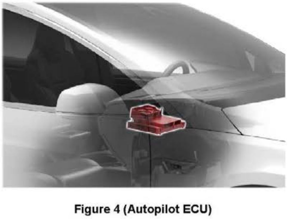
FIRST PICTURES - Tesla Autopilot 2.0 ECU (Nvidia PX 2)
- Thread starter lunitiks
- Start date
LargeHamCollider
Battery cells != scalable
Not conclusive, but it is suggestive.Size and number of inputs.
S4WRXTTCS
Well-Known Member
No way, we got the very first pictures in this thread: The module location, the enclosure shape, size and measurements, cooling type, in- and output connectors etc. Still waiting for the teardown, yes, but hey what can you do
stopcrazypp
Well-Known Member
That shows the single SoC configuration. Tesla is using the double SoC configuration. Nvidia however suggested two PX2 double chip boards are required for fully autonomous driving and that Tesla's configuration is only sufficient for "autochauffeur".At 9:59 the slide shows that px2 is only sufficient for L3 autonomy?
Autonomous Car Development Platform from NVIDIA DRIVE PX2
Tesla is using the double SoC configuration
And you know that for a fact how? All we know for sure is that Tesla is not using the NVida designed boards, they made a custom one. So we have no idea how many chips are on it.
JeffK
Well-Known Member
Saying something is "sufficient" is an unknown at this point since there are no true lvl 5 cars on the road.At 9:59 the slide shows that px2 is only sufficient for L3 autonomy?
Nvidia is not even saying you'd need two for fully autonomous, they are suggesting you can put more than one in a vehicle...two, five, ten, whatever.
I've also never seen a source suggesting Tesla's Drive PX2 is custom. Custom in the sense that a PNY or MSI Geforce GTX 1080ti is "custom" vs the Nvidia reference card or did Tesla help design it? Is it simply custom connectors? We know they wanted a custom setup with EyeQ3 but they couldn't get it, I don't know any more than that.
stopcrazypp
Well-Known Member
Okay, maybe they are using a "custom" double SoC board. But either way, they definitely aren't using the small board in that picture.And you know that for a fact how? All we know for sure is that Tesla is not using the NVida designed boards, they made a custom one. So we have no idea how many chips are on it.
double SoC board
Again, how do you know it is a double SoC board?
JeffK
Well-Known Member
The non-small form factor Drive PX2 "system" consists of two SoCs and two GPUs and it's the same approximate shape as the enclosure in the AP 2.0 cars. Until someone opens one up, most of us are assuming it's not full of empty space.Again, how do you know it is a double SoC board?
If they were using anything radically different then you can't really call it Drive PX2 anymore. It *should* be two Tegra (Parker) chips and two GPUs (Pascal)
(where small form factor is one and one)
Last edited:
The non-small form factor Drive PX2 "system" consists of two SoCs and two GPUs and it's the same approximate shape as the enclosure in the AP 2.0 cars. Until someone opens one up, most of us are assuming it's not full of empty space.
A bunch of that space is necessary for all of the connectors. And more of it is necessary for cooling since Tesla didn't go with a liquid cooled setup.
JeffK
Well-Known Member
But the connectors are outside the box and cooling is likely happening with those black sections on the top:A bunch of that space is necessary for all of the connectors. And more of it is necessary for cooling since Tesla didn't go with a liquid cooled setup.

stopcrazypp
Well-Known Member
Not 100% sure yet, but so far in the other thread there are two nodes in HW2, one called "ape" (which seems to handle EAP) and one called "lb". HW1 only had 1 node.Again, how do you know it is a double SoC board?
BTW, HW2 systems added 2 more computer systems (As in network-accessible) compared to HW1, one is eap itself, the other one is cryptically labeled lb, but I have no idea what is it and when is it on if ever.
Anyway important parts - for lb I only know the name and adress, but it's not on ever as far as I can tell.
the diagram noting A-B link is gige seems to imply B host is a separate node, so a high candidate for this LB stuff.
EAP node is actually called ape.
They appear to be network connected just like how PX2 describes the double SoC configuration:
AP2.0 Cameras: Capabilities and Limitations?
The "ape" part is already confirmed to match the Parker SoC configuration (used in PX2):
AP2.0 Cameras: Capabilities and Limitations?
"lb" doesn't appear active, so can't verify yet.
Last edited:
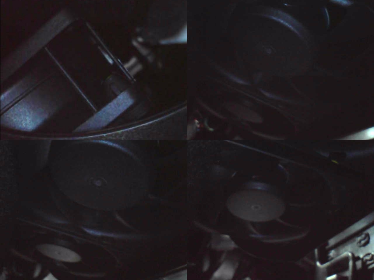
An illustration of the AP2ECU assembly just came out on Teslas service site. Poor quality but it is what it is:
Notice the non-centered placement of the cooling fans.
Source (see page 24)
Notice the non-centered placement of the cooling fans.
Source (see page 24)
Last edited:
petergrub
Member
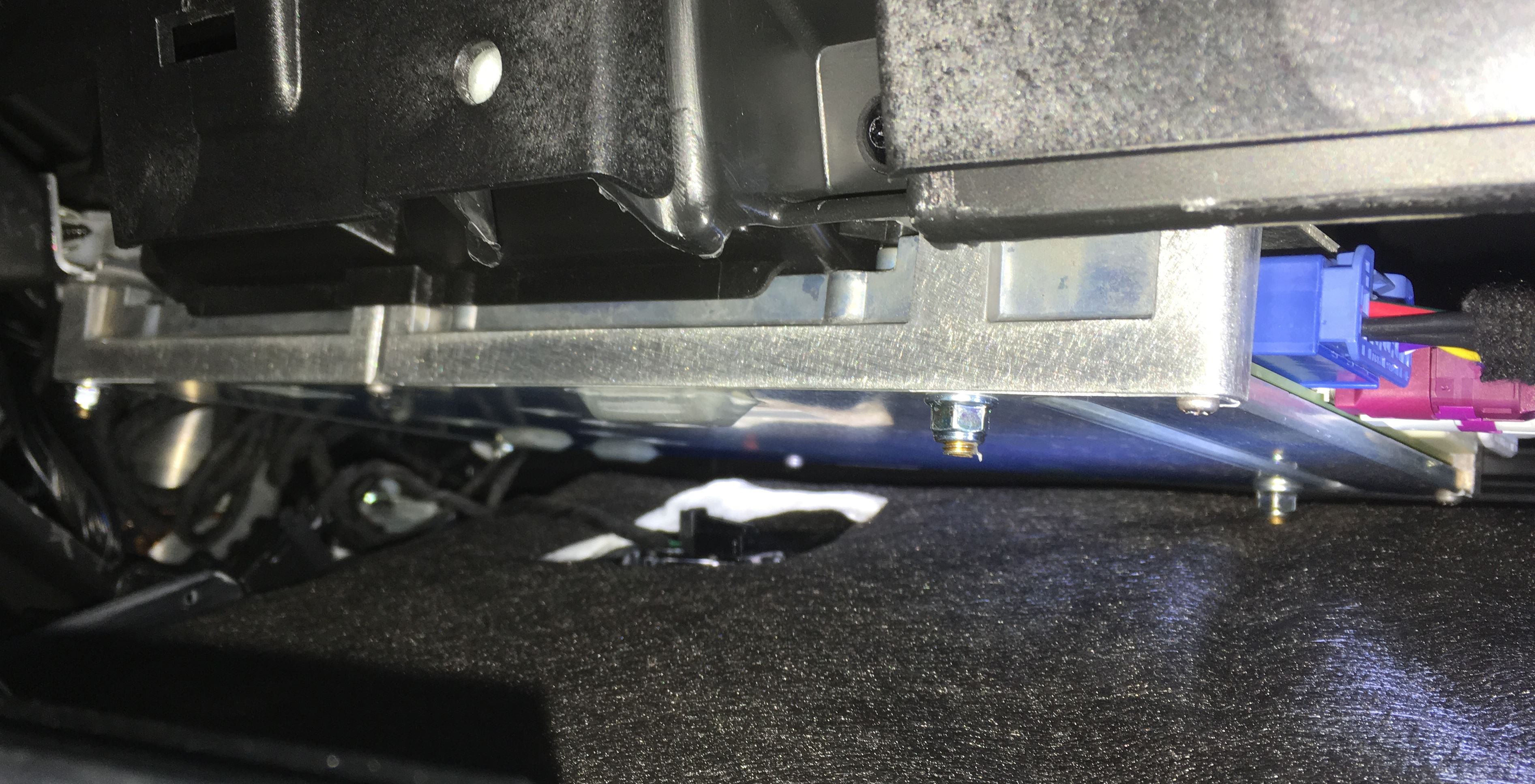
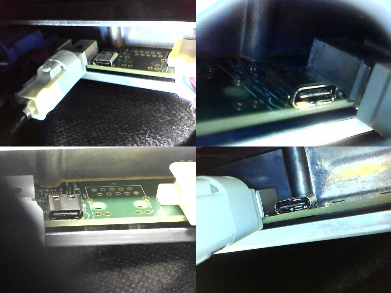
I just took pictures inside the Autopilot ECU and found this thread. Seems you all have been looking for these pictures. Enjoy.
Model S Autopilot ECU
Glamour shots
View media item 118069View media item 118064
Model S Autopilot ECU
Glamour shots
View media item 118069View media item 118064
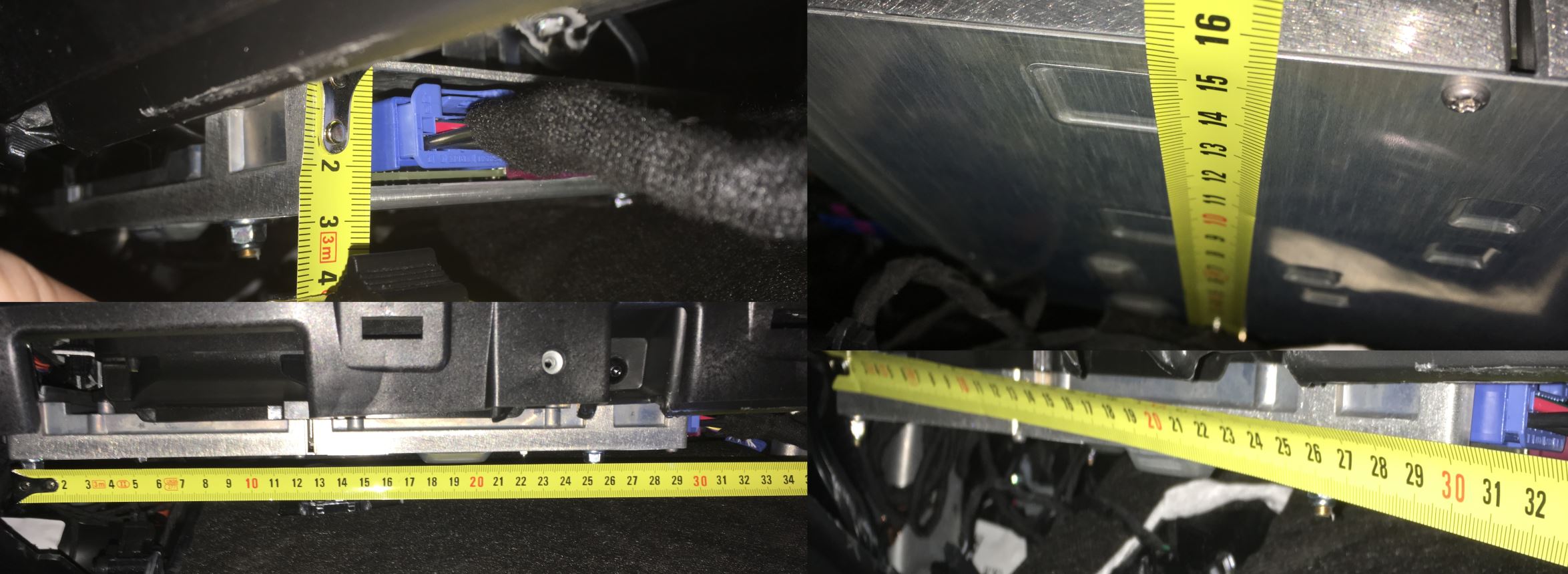
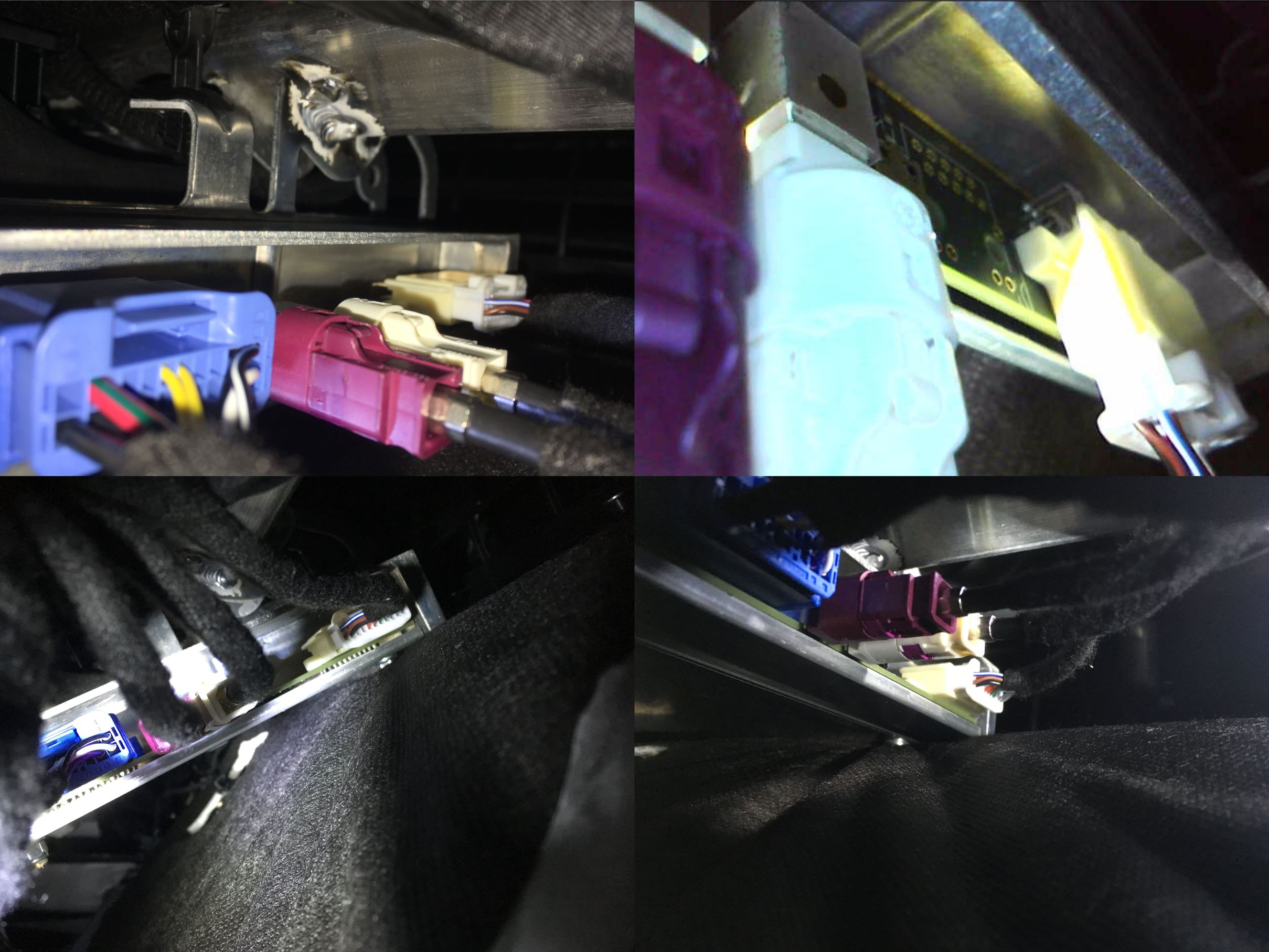
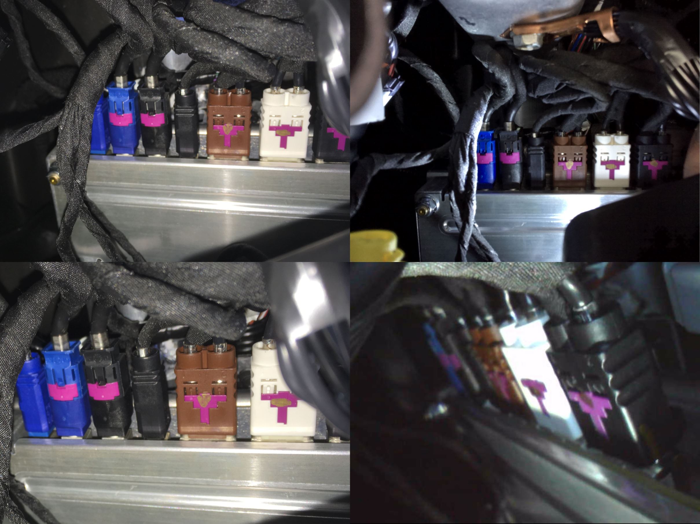
How do you think: would it be possible to fit this one instead of AP1?With a little help from my friend w/AP2, I just captured some nice pics of the AP2.0ECU! Managed to do some measurements to(metric):
Now - someone with the b**** please unscrew that thing and open it for us to see its guts
Similar threads
- Replies
- 465
- Views
- 32K
- Replies
- 141
- Views
- 35K
- Replies
- 193
- Views
- 75K
- Replies
- 86
- Views
- 37K